A Ghost in the Machine
In the world of classical physics—the world of billiard balls and falling apples—energy is a strict barrier. If you throw a ball at a thick concrete wall, it will bounce back 100% of the time. But in the Quantum World, particles like electrons behave like waves of probability.
If the wall is thin enough (at the nanometer scale) and the electron is “energetic” enough, there is a non-zero mathematical probability that the electron will effectively vanish on one side and reappear on the other. It doesn’t “break” the wall; it simply tunnels through it. This is Quantum Tunneling, and without it, your smartphone and laptop wouldn’t have any storage.
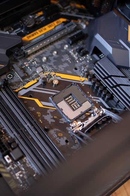
The Architecture of NAND Flash
To understand how SSDs use this “ghostly” behavior, we have to look inside a NAND Flash cell. Specifically, the Floating Gate Transistor.
The Transistor Layout:
- Control Gate: The “switch” where we apply voltage.
- Floating Gate: The “bucket” where electrons are stored. It is surrounded by an insulating oxide layer.
- Oxide Layer (The Wall): This is the thin barrier that holds the electrons in place.
       [ Control Gate ]
------------------------------ <--- Isolation Layer
       [ Floating Gate ]  <--- (Electrons stay here)
------------------------------ <--- Oxide Layer (THE BARRIER)
        [ Substrate ]
1. Programming: Fowler-Nordheim Tunneling
When you “write” a file, the SSD controller applies a high-voltage pulse to the Control Gate. This creates a strong electric field that narrows the potential energy barrier of the oxide layer.
Through a process called Fowler-Nordheim (FN) Tunneling, electrons from the substrate “tunnel” through the oxide wall and get trapped in the Floating Gate. Once the voltage is removed, the barrier becomes too wide again, and the electrons are stuck—potentially for decades.
- Logic 1: Floating gate is empty.
- Logic 0: Floating gate is full of electrons.
2. Floating Gate vs. Charge Trap Flash
As SSDs get smaller, the Floating Gate architecture faces limits (it’s bulky). Modern “3D NAND” often uses Charge Trap Flash (CTF).
| Feature | Floating Gate | Charge Trap |
|---|---|---|
| Mechanism | Poly-silicon gate stores charge. | Non-conductive silicon nitride layer traps charge. |
| Scalability | Hard to shrink; thick. | Very thin; allows for 200+ layers. |
| Durability | Higher data retention. | Faster programming; less interference. |
3. The Downside: Quantum Wear and Tear
Every time an electron tunnels through the oxide layer, it causes microscopic, irreversible damage to the chemical structure of the insulator. This is known as Trap-Assisted Tunneling.
Eventually, the “oxide wall” becomes so swiss-cheesed with defects that electrons can leak back out through a process called SILC (Stress-Induced Leakage Current). This is why SSDs have a TBW (Terabytes Written) limit. Once the gate becomes “leaky,” the cell can no longer hold its charge, and you get Bit Rot.
4. Why Temperature Matters
Quantum tunneling is sensitive to heat. At high temperatures, the oxide barrier vibrated, making it even easier for trapped electrons to “escape” or tunnel back out. This is why SSDs left in a hot car can lose data much faster than those kept in a cool data center.
Conclusion
The next time you save a high-resolution photo or a 100GB game, pause for a moment. You are witnessing the mastery of quantum mechanics. We have taken the most bizarre “forbidden” laws of subatomic physics and used them to build the most reliable filing cabinet in human history.
References & Further Reading
- IEEE Xplore: Physics of NAND Flash Memory Basics
- Samsung Semiconductor: How V-NAND Technology Works
- Richard Feynman: The Character of Physical Law (Quantum Section)
- Tom’s Hardware: SSD Endurance and the Physics of Flash